bare_die.jpg

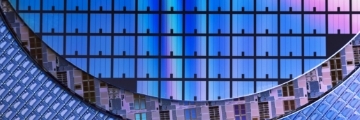
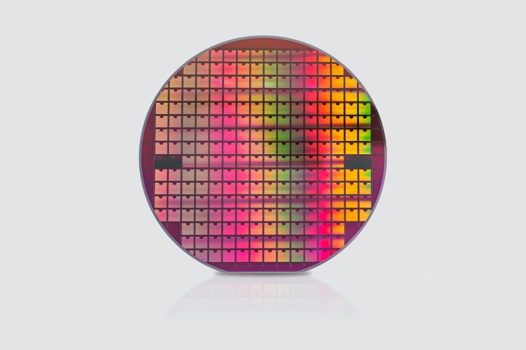
Power Device Wafer/Bare die -

Si IGBT Bare Die

Main Features
  • Low switching loss
  • Hi switching speed
  • Excellent cost performance
  • Latest Trench structure design
  • Pairable with Si-FRD/SiC-SBD
  • Automotive/Industrial applications
  • PPAP available

Product info

Si IGBT Bare Die is the result of the Actron Group's semiconductor vertical integration capabilities, which leverages its own professional chip design department and collaborates with upstream substrate manufacturing/epitaxial growth/Fab from the group to develop Si IGBT power device wafers/bare die. The highly versatile and output-stable product combination is suitable for various discrete power devices and power modules.

Model No. Voltage Current Wafer Size Packaging FSM BSM
Si_TBD 650V - 6" or 8" Unsawn wafer Sawn wafer on frame Chip on tray Tape & Reel Al AlCu Solderable Ti/Ni/Ag Ti/NiV/Ag Ti/Ni/Au
Si_TBD 750V - 6" or 8" Unsawn wafer Sawn wafer on frame Chip on tray Tape & Reel Al AlCu Solderable Ti/Ni/Ag Ti/NiV/Ag Ti/Ni/Au
Si_TBD 1200V - 6" or 8" Unsawn wafer Sawn wafer on frame Chip on tray Tape & Reel Al AlCu Solderable Ti/Ni/Ag Ti/NiV/Ag Ti/Ni/Au